Overview
Our research objective is to study functional materials in forms of thin films and nanostructures for electronic and photonic applications, ranging from material synthesis and characterization, property measurement, to device fabrication. The research work is currently focused on metal oxide and metal based materials in two major applications:
- Energy harvesting devices like solar cells and photo-electrochemical cells
- Energy-efficient devices such as smart devices, sensors, and light-emitting devices.
Nanoscale Smart Devices
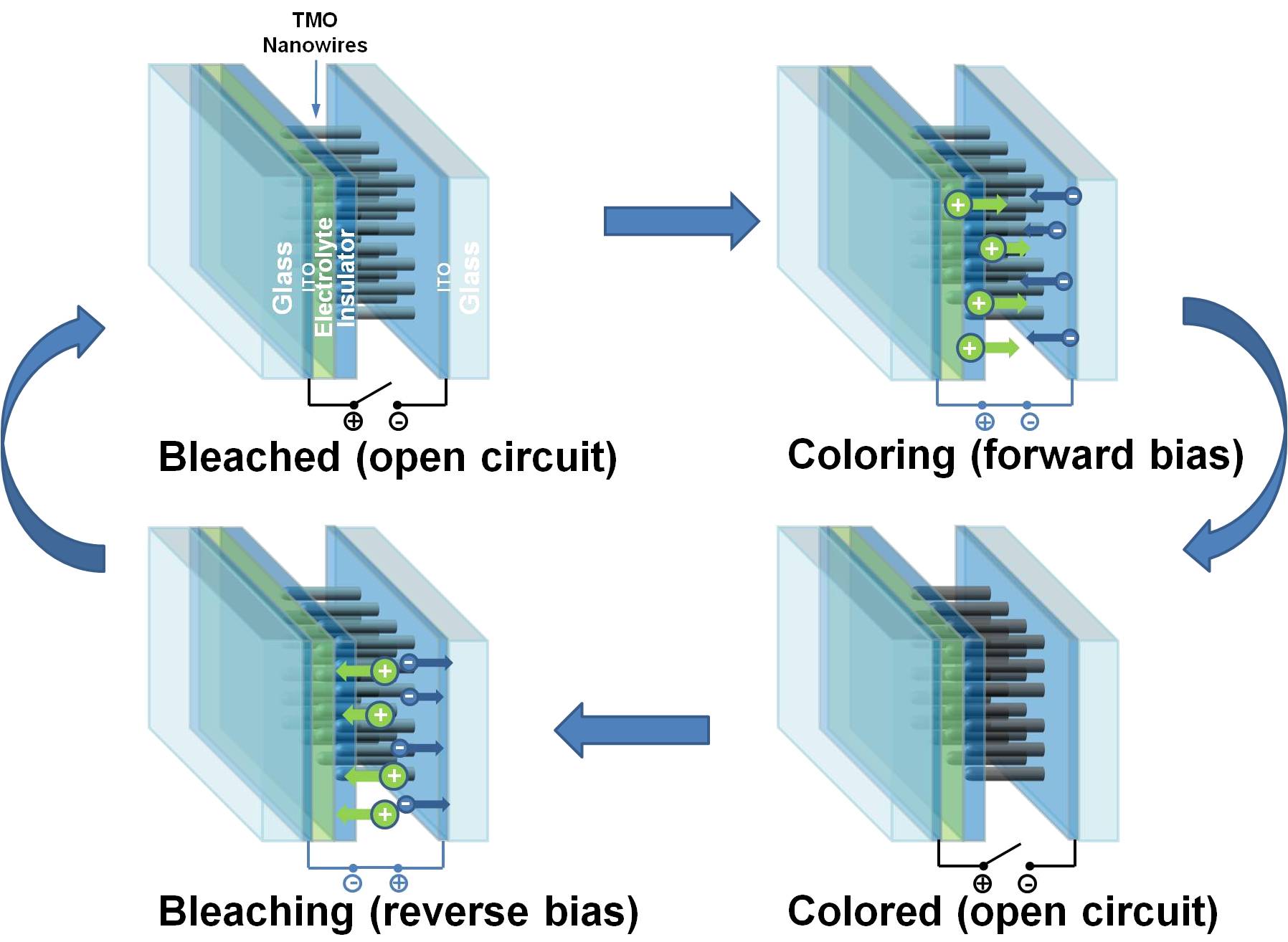
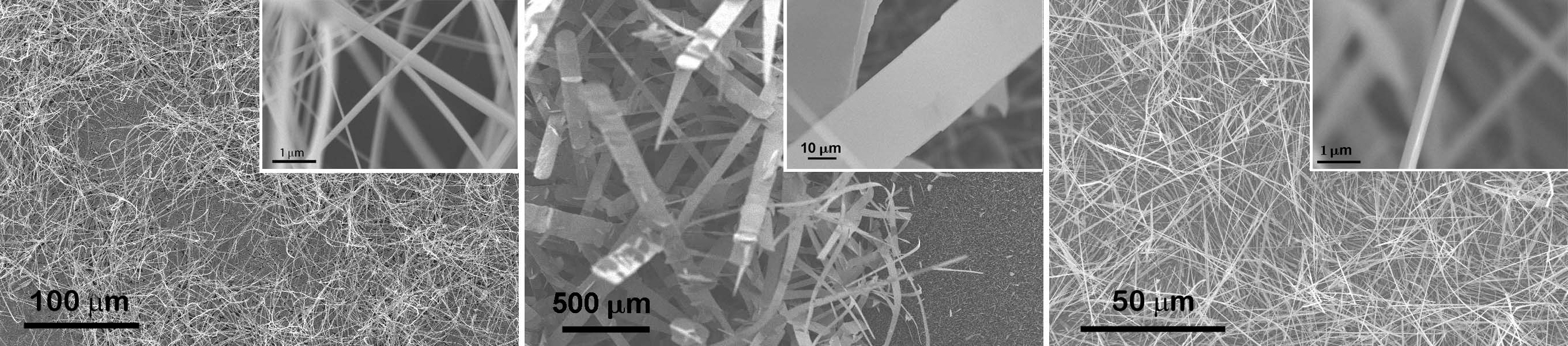
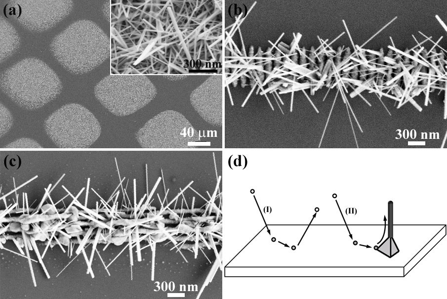
Chromic materials are capable of changing their color reversibly in response to external stimuli, such as electric field (electrochromism), light (photochromism), heat (thermochromism), and pressure (piezochromism), etc. They have important applications in smart devices with high energy efficiency. We have developed 1D nanostructures of transition metal oxides including WO3, MoO3, and V2O5 (JVST B, 28, 310, 2010). Compared to thin films of oxides, 1D nanostructures are expected to have enhanced response speed and coloration efficiency with their small dimensions and high material qualities.
* This material is based upon work supported by the National Science Foundation under Grant No. DMR-1006547. Any opinions, findings and conclusions or recommendations expressed in this material are those of the author(s) and do not necessarily reflect the views of the National Science Foundation (NSF).
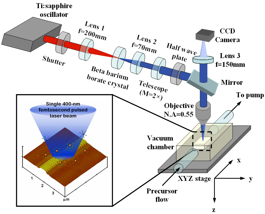
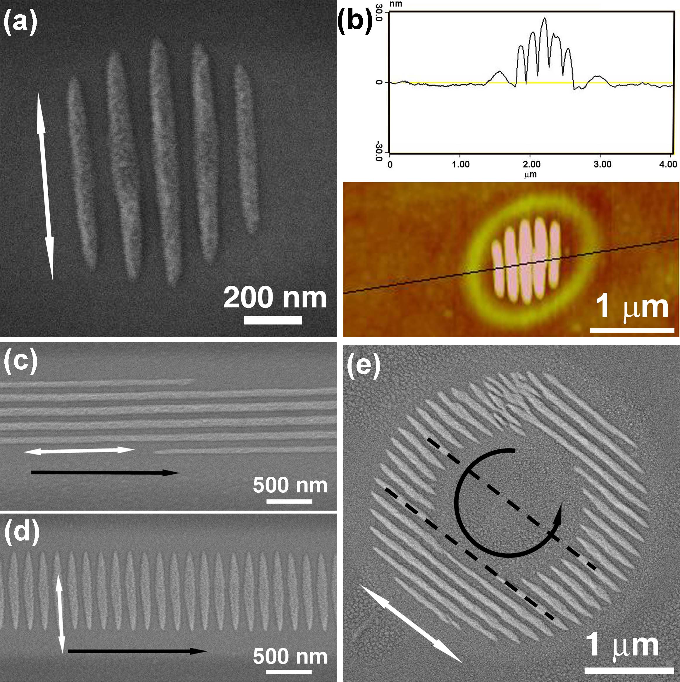
Metal Nanogratings
Laser-induced chemical vapor deposition (LCVD) using a laser beam (photons) to initiate the localized deposition is an important add-on direct-write technique for nanoscale patterning. We have developed tungsten nanogratings with sub-100 nm linewidths and subwavelength periods with a single 400-nm femtosecond laser beam without beam shaping using LCVD (Opt. Express 15 (10), 5937, 2007.). This project is a collaboration with Prof. Tsing-hua Her in Department of Physics and Optical Science.