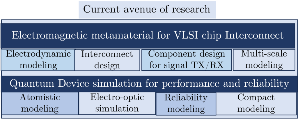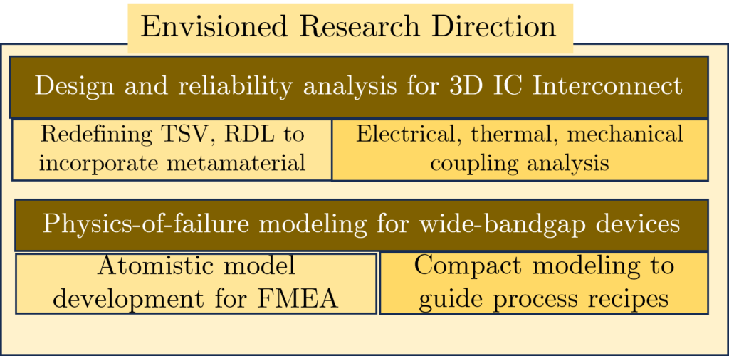
The Information Age has witnessed remarkable advancements in the past five decades, impacting various spheres of society. Moore’s Law, which has guided these advancements, may soon reach its limits as lithography approaches atomic scales. Consequently, the semiconductor industry is embracing innovative chip design approaches, including high-density, heterogeneous chiplet integration, and 2.5D/3D monolithic IC integration. To keep pushing the frontier of semiconductor device and electromagnetic research in post-Moore era, my research lab envision to drive my research in two avenues:
1. Modeling and Design of electromagnetic metamaterials for VLSI Interconnect Technology:
Electromagnetic metamaterials, characterized by unconventional electromagnetic properties not found in natural media can be engineered to design high-performance device that can overcome standard physical limits. For ultra-short distance (1 micron to 1cm) data transfer among chips, our laboratory aims to drive research on novel electromagnetic material for signal propagation in advanced VLSI chip packaging technology.
2. Modeling of Nanoelectronic Device for Performance and Reliability Analysis:
For burgeoning Silicon-alternative technologies, such as high power III-V devices for power electronics and RF communication, which suffers greatly from the issue of reliability, our research laboratory aims to drive nanoelectronic device research for its performance and reliability improvement for high performance, high bandwidth, and energy-efficient power delivery and signal amplification.